Get in touch

Contact SMIC to discuss facilities and partnerships.

Email SMIC
25 March 2020

How transmission electron microscopy can improve product performance

Transmission electron microscopy (TEM) is a powerful technique for observing and analysing the microstructure of materials, generating highly-magnified images at a sub-nano scale. Here at the Sheffield Multimodal Imaging Centre, we’re using TEM to study and improve the performance of steel products and hard coatings.

A unique tool

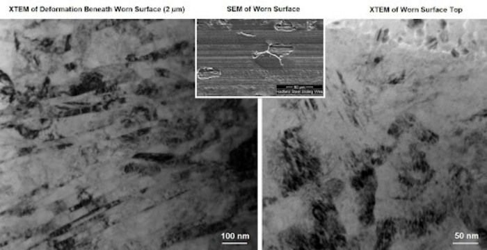
Wear as a result of sliding/impacting is caused by changes in a material’s microstructure at an atomic level.TEM is the only method capable of observing these changes.

This means it can be used to investigate the cause of failure of a product or mechanism. It’s been applied to cutting tools, railway tracks, mining equipment and many other areas.

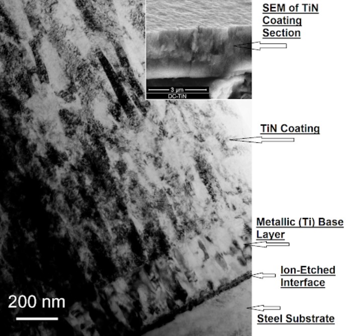
Physical vapour deposition (PVD) hard coatings are widely used in high-performance machining tools, making them more durable and scratch resistant. Because of the nanoscale structures used in these coatings, TEM is an essential tool in developing and understanding them.

Preparing the sample

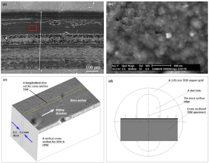
Sample preparation plays a key role in TEM. A sample must be thin enough to allow electrons to pass through it, usually a thickness of a few tens of nanometres. 

For the examples below, cross-sectional specimens were prepared using specialist equipment. Figure 1 shows how a cross-sectional specimen of a worn surface sample is typically prepared. 

Cross-sectional TEM sample preparation
Figure 1: The procedure of cross-sectional TEM sample preparation: (a) A ball-on-disc wear scar; (b) Fine features of a tribofilm attached on the worn surface; (c) A schematic 3D view of a worn surface sample showing several means of examinations; (d) A schematic view of a cross-sectional foil specimen ready for ion-beam polishing.
A transmission electron microscopy image of the worn surface of steel
Figure 2: Cross-sectional TEM of the worn surface microstructure of austenitic Hadfield steel: (Left) The nano-laminate microstructure showing severe plastic deformation; (as shown in the SEM image, insert in upper middle); (Right) Nano-equaxial grain and nano-twins immediately below the worn surface.

Optimising Hadfield steel

High-strength Hadfield steel is widely used in wear resistant and impact-resistant mining and railway parts. In order to optimise and improve performance, it’s important to measure and understand how the material wears.

We carried out a dry sliding wear test on Hadfield steel to evaluate its friction and wear properties. Scanning electron microscopy (SEM) revealed severe deformation, hardening, and spalling detachments (where the material breaks off in fragments) of the worn surface. Cross-sectional TEM observation shows the deformation induced microstructure changes, shown in Figure 2.

The results suggest that the hardening and deformation induced a reduction in the size of the grains inside the material. This made the worn surface brittle, which caused the spalling wear – the main reason for material failure.

A transmission electron microscopy image of the worn surface of steel
Figure 3: The worn surface of austempered 300M steel, showing a gradient microstructure of (I) laminates just below the worn surface, (II) a shearing-deformed zone upon (III) the normal bainitic/martensitic microstructure.

Analysing coatings

Transition metal nitride (e.g TiN) coatings grown by PVD normally have a column-like structure. The coating properties are dependent on the coating deposition conditions which have a strong influence on the microstructure, in turn influencing coating performance. 

Figure 4 shows cross-sectional microstructure of a TiN coating grown by direct-current magnetron sputtering – a fast technique for applying a thin coating on a surface. The SEM image shows the surface and a fractured section of the coating in 3D. The TEM image reveals the microstructure of the coating: (from bottom to upper part) an ion-etching modified interface, a metallic (Ti) base layer, and the columnar TiN coating.

Using TEM, researchers can visualise and analyse the coating’s microstructure, then establish a link between the deposition conditions, the micro-structure and its performance. From this, significant improvements to the coating can be made.

A scanning electron microscopy image of a metal coating
Figure 4: Cross-sectional microstructure of DC magnetron sputtered TiN coating (insert is SEM of fracture surface through coating).

Get in touch

Contact SMIC to discuss facilities and partnerships.

Email SMIC