Atomic Force Microscopy (AFM) is a high-resolution imaging technique that uses an extremely fine probe to scan the surface of a sample and create a detailed three-dimensional map at the nanometre scale. By physically measuring the surface, AFM can provide quantitative information about topography, roughness, feature dimensions, surface defects, adhesion, friction and local mechanical properties. It is particularly valuable for analysing coatings, polymers, composites, thin films, functional surfaces and advanced materials containing features below the resolution limit of conventional optical microscopy.
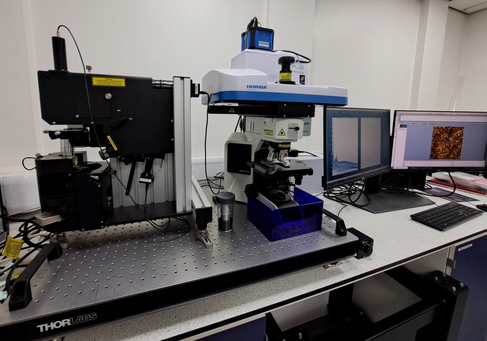
The integrated HORIBA XploRA™ confocal Raman microscope and OmegaScope™ Atomic Force Microscope (AFM) provides a powerful platform for understanding materials by combining chemical analysis with nanoscale surface characterisation. The system allows researchers to investigate not only the chemical fingerprint of a material but also its surface structure at nanoscale.
The strength of the HORIBA XploRA–OmegaScope combination lies in its ability to correlate chemistry and morphology on exactly the same area of a sample. A particle, coating defect, wear track, contaminant or nanoscale feature identified by AFM can be chemically characterised by Raman spectroscopy, while Raman-derived compositional differences can be directly related to changes in surface structure measured by AFM. The OmegaScope platform has been specifically designed for coupled AFM-optical measurements, providing high-resolution AFM imaging alongside Raman, photoluminescence and fluorescence analysis.
This capability is particularly useful for addressing real-world research and industrial challenges, including:
- Characterisation of advanced coatings and surface treatments
- Investigating additive manufacturing materials and defects
- Analysing polymer blends, composites and nanocomposites
- Examining battery and energy-storage materials
- Studying biomaterials and medical device surfaces
- Failure analysis of electronic and engineering components
- Identifying contaminants, inclusions and wear products
- Linking material processing conditions to microstructural performance
By combining nanoscale topographical information with detailed chemical and structural analysis, the AFM-Raman facility helps researchers and industrial partners gain a more complete understanding of their materials than would be possible with either technique alone. Whether supporting fundamental research, product development, process optimisation or failure investigation, our specialists can work with clients to design analytical programmes that deliver meaningful and actionable insights.