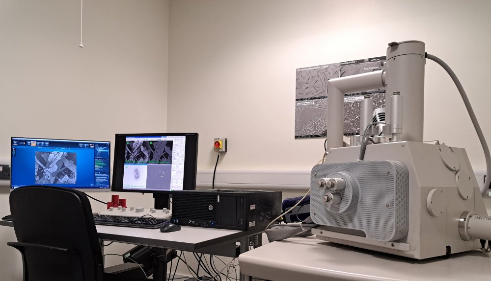
SEM is one of the most useful tools available to materials scientists.
In SEM operation, the sample is put in the vacuum chamber of the microscope and a fine beam of high energy electrons is scanned across a small area. During the scan, interactions between the incident electron beam and the sample surface lead to several types of emissions, including secondary electrons, back-scattered electrons, and characteristic X-rays.
Emissions are detected by different detectors to produce several imaging modes
- the secondary electron image for the surface morphology of the scanned area
- the back-scattered electron image for compositional mass profile
- the characteristic X-rays for energy dispersive spectroscopic chemical analysis.
SEM is a very versatile analytical instrument having up to nm-scale spatial resolution. Analytical SEM is extensively used in various types of materials characterisation and failure investigations.
Why SEM is so useful
- It can give wide range of magnifications from 100× to 100,000× or even higher depending on sample material and the instrumental spatial resolution
- SEM has great depth-of-focus which allows imaging of rough surfaces such as fractures, as-machined surfaces, corrosion and wear of materials, micro-/nano-scale particles, etc
- With little or no need of sample preparation, a wide range of materials can be analysed on SEM, eg conductive/semi-conductive/insulating materials, particles/fibres/blades, various types of coatings, thin films and surfaces